A featured contribution from Leadership Perspectives: a curated forum reserved for leaders nominated by our subscribers and vetted by our editorial board.

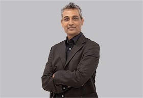
Navin is a seasoned semiconductor and engineering leader, where he oversees business operations in India and leads Central Engineering. He has deep experience in custom ASIC design for infrastructure domains including networking, processors, cloud, automotive, and AI/ML applications. Earlier, he worked with IBM, Freescale, Cadence, and Texas Instruments across automotive, consumer, and chip design roles. He holds a degree in Electronics and Communication from NIT Surathkal and has played an active role in strengthening India’s semiconductor ecosystem through industry forums, advisory committees, and skilling initiatives.
As India expands its AI and semiconductor ambitions, the focus is shifting from building traditional data centers to solving the deeper challenge of efficient data movement between compute, memory, and storage. Global trends in chiplets, advanced packaging, and energy-aware computing are redefining how AI infrastructure is designed and deployed. Against this backdrop, India has an opportunity to rethink infrastructure as integrated ‘intelligence centers’ powered by renewable energy and distributed systems.
1.How can India turn the data movement crisis into a national advantage by building ‘Intelligence Centers’ that combine advanced memory packaging, sovereign compute, and renewable energy rather than copying standard data centers?
India has a unique opportunity to rethink AI infrastructure from first principles rather than replicate legacy hyperscale models. The real constraint in AI today is not compute alone, but the inefficiency of moving data between memory, compute, and storage layers. We can reframe this by building ‘intelligence centers’ that tightly integrate compute, memory, and advanced packaging. This is where advanced packaging, especially chiplet- based architectures and 2.5D/3D integration- becomes critical, as it enables higher bandwidth, lower latency, and better energy efficiency at the system level.
India can differentiate by co-optimizing infrastructure with renewable energy and data locality, creating more distributed and energy-aware compute clusters. This approach aligns well with India’s scale and diversity, and can help us leapfrog traditional data center designs rather than follow them.
2. Beyond HBM and packaging, which radical chip memory architectures or data flow paradigms (in memory computing, optical interconnects, neuromorphic chips, etc.) should Indian fabless firms and labs pioneer to bypass legacy bottlenecks and offer differentiated AI hardware?
India should focus on areas where system-level innovation can bypass legacy bottlenecks rather than competing directly in saturated domains. Three promising directions stand out:
- In-memory and near-memory computing, which significantly reduces data-movement overhead
- Optical interconnects and photonics, which provide high-bandwidth, low-latency communication at scale
- Chiplet architectures, enabling modular design and heterogeneous integration across nodes and technologies
Additionally, areas like neuromorphic and domain-specific accelerators offer long-term potential, particularly when aligned with India’s research strengths. The key is not picking a single technology, but building capabilities across design, packaging, and system integration so that India can innovate at the architecture level, not just at the component level.
3. What new education and skilling frameworks in materials, process integration, advanced packaging, and AI hardware co design must India build so future engineers become originators of solutions to the data movement crisis?
The semiconductor workforce of the future will be inherently multidisciplinary. India needs to move from siloed engineering education to integrated programs spanning materials, device physics, process engineering, packaging, and system architecture, coupled with strong exposure to AI and software. Three shifts are critical:
- Hands-on, lab-driven learning aligned with industry challenges, not just theory
- Co-development models between academia and industry, enabling students to work on real problems early
- Specialized tracks in advanced packaging, system integration, and AI-hardware co-design, which are currently underdeveloped
If we get this right, India can move from being a provider of talent to becoming a creator of deep technology.
Also Read: Can India Become America's Trusted Chip Partner?
4. Facing export controls and concentrated memory production, how should India align the ISM, ATMP investments, and international partnerships to secure strategic autonomy in HBM and advanced packaging without creating fresh dependencies?
India’s approach should be anchored in building selective depth while maintaining strong global partnerships. Rather than trying to replicate the entire stack, India should focus on areas where it can build differentiated strengths- particularly in advanced packaging, design, and integration- while collaborating globally for upstream technologies like memory. Alignment between ISM, OSAT investments, and industry demand is critical. We should also ensure that ecosystem development spans materials, equipment, and process capabilities, reducing long-term dependencies.
Strategic autonomy in this context is not isolation, it is the ability to participate meaningfully in global supply chains with trusted and resilient capabilities.
India has a unique opportunity to rethink AI infrastructure from first principles rather than replicate legacy hyperscale models.
5. As India scales intelligence infrastructure, how can it ensure inclusive prosperity meeting energy and sustainability goals, democratizing sovereign AI access, and preventing a wider digital divide?
As India scales its AI infrastructure, it is important to balance performance with sustainability and accessibility. This includes:
- Designing energy-efficient systems, leveraging innovations in packaging and system architecture
- Integrating renewable energy into data infrastructure
- Enabling distributed access to compute, so innovation is not limited to a few large players
Equally important is building open ecosystems- through academia, startups, and industry collaboration- so that access to AI tools and infrastructure is democratized. India’s advantage lies in its ability to combine scale with inclusion. If done well, we can build not just large infrastructure, but equitable infrastructure that supports broad-based innovation.
In essence, the Indian AI and semiconductor sector’s growth, however, is about to undergo a new phase of transformation from one that focuses on increasing the compute capability to making the data movement more efficient across different levels of memory, storage, and processors. In light of the emerging global trends such as chiplet architectures, advanced packaging technologies, optical interconnections, and energy-efficient computing systems, the need is less about scaling but more about the intelligence in the design and connectivity of systems.
It offers a much broader scope for India to leverage design, material, energy, and talent to shape future infrastructure ecosystems differently. It would enable the country to become not just a manufacturing or services center but also to contribute towards innovation in AI system architecture if this convergence comes through. The future progress, however, depends on creating efficient computing systems.